How to Reduce Noise in PCB Design
Video Contents, by time-offset
0:00 Intro
0:43 What is Noise in a PCB?
1:17 PCB Noise Reduction Strategies Overview
3:22 Filtering
7:48 Shielding
11:41 Advanced Noise Reduction Options
16:45 Isolation and Splitting Ground Planes
PCB Design: Electronic Noise Filtering
Electronic noise filtering in PCB (Printed Circuit Board) design is a critical aspect, especially in sensitive electronic systems where noise interference can degrade performance or cause malfunctions. Here’s a brief overview of noise filtering in PCB design:
1. Understanding Noise Sources: Before implementing any filtering techniques, it’s essential to identify the sources of noise in the system. Common sources include electromagnetic interference (EMI) from external sources, switching noise from digital components, power supply ripple, and ground loop interference.
2. Layout Considerations: Proper PCB layout design plays a significant role in minimizing noise. Techniques such as separating analog and digital components, routing high-speed signal traces away from sensitive areas, and employing a star grounding scheme can help reduce noise coupling.
3. Component Selection: Choosing components with built-in noise suppression features can simplify filtering requirements. For example, using bypass capacitors across power supply lines and decoupling capacitors near ICs can help mitigate high-frequency noise.
4. Bypass and Decoupling Capacitors: Placing bypass and decoupling capacitors strategically across power and ground planes helps filter out high-frequency noise and stabilize voltage levels. These capacitors provide a low-impedance path for high-frequency noise to ground, preventing it from affecting the rest of the circuit.
5. Ferrite Beads and Inductors: Ferrite beads and inductors are commonly used to attenuate high-frequency noise. Placing them in series with signal lines or power supply lines helps block unwanted noise while allowing the desired signals to pass through.
6. Grounding Techniques: Proper grounding is crucial for noise reduction. Implementing a solid ground plane, minimizing ground loops, and using separate analog and digital ground planes can help prevent noise coupling between different parts of the circuit.
7. Shielding: Enclosing sensitive components or signal traces within a shielded enclosure or using shielded cables can protect against external electromagnetic interference.
8. Filtering Circuits: For more advanced noise filtering requirements, dedicated filtering circuits such as RC filters, LC filters, or active filters can be implemented. These circuits selectively attenuate noise at specific frequencies while allowing desired signals to pass through relatively unaffected.
9. Simulation and Testing: It’s essential to simulate and test the effectiveness of noise filtering techniques during the PCB design phase. Tools like SPICE simulation software can help evaluate the performance of filtering circuits, while real-world testing with oscilloscopes and spectrum analyzers verifies noise suppression in the final PCB prototype.
By incorporating these noise filtering techniques into the PCB design process, designers can effectively mitigate noise interference and ensure optimal performance and reliability of electronic systems.
PCB Design: Electronic Noise Shielding
When designing a PCB to shield against noise, there are several strategies you can employ to minimize electromagnetic interference (EMI) and maintain signal integrity:
1. Ground Planes: Implementing solid ground planes on both sides of the PCB can help minimize noise by providing a low-impedance path to ground for high-frequency signals. Ensure that the ground plane is uninterrupted and connected to the chassis ground.
2. Partitioning: Physically separate noisy components, such as switching power supplies or high-speed digital circuits, from sensitive analog components to prevent noise coupling. Partitioning the PCB into separate sections for analog and digital circuits can help minimize interference.
3. Shielding Enclosures: Use metal enclosures or shields to physically isolate sensitive components or sections of the PCB from external sources of EMI. Shielding enclosures can be grounded to provide additional protection against electromagnetic radiation.
4. Signal Routing: Route high-speed signal traces away from sensitive components and keep them as short as possible to reduce the loop area and minimize radiation. Use differential signaling for noise-sensitive connections to improve noise immunity.
5. Filtering Components: Incorporate filtering components such as ferrite beads, inductors, and capacitors into the PCB design to suppress high-frequency noise. Place these components strategically on signal lines and power rails to attenuate unwanted noise.
6. Transmission Line Techniques: Employ transmission line techniques such as controlled impedance routing to minimize signal reflections and crosstalk, which can contribute to EMI. Match the characteristic impedance of transmission lines to the source and load impedance to optimize signal integrity.
7. Component Placement: Carefully place components on the PCB to minimize the length of signal traces and reduce the loop area of sensitive circuits. Group components with similar functions together and avoid routing high-speed signals near sensitive analog components.
8. Grounding Scheme: Implement a robust grounding scheme to ensure proper grounding of all components and minimize ground loops. Use star grounding or hierarchical grounding techniques to maintain a clean ground reference and reduce ground bounce.
9. Shielded Cables: Use shielded cables for external connections to further reduce susceptibility to EMI from external sources. Ground the shields at both ends to provide effective shielding against electromagnetic radiation.
10. Simulation and Testing: Use simulation tools to analyze the electromagnetic compatibility (EMC) of the PCB design and identify potential sources of EMI. Perform EMC testing on prototype PCBs to verify compliance with regulatory standards and ensure effective noise shielding.
By implementing these noise shielding techniques during the PCB design process, you can minimize electromagnetic interference and maintain signal integrity in electronic systems.
PCB Design: Isolation of components and signal source/return paths
Isolating components and controlling signal source/return paths are crucial aspects of PCB design to minimize noise and ensure signal integrity. Here are some strategies to achieve effective isolation and routing:
1. Component Placement: Physically separating noisy components (such as switching power supplies, clock generators, or high-speed digital circuits) from sensitive components (such as analog circuits) helps reduce interference. Place components strategically on the PCB layout to minimize the interaction between them and to keep signal paths as short as possible.
2. Ground Planes: Implement separate ground planes for different sections of the PCB, especially for analog and digital circuits. This helps prevent noise coupling between different parts of the circuit. Ensure that ground planes are continuous and connect them to the chassis ground for effective shielding.
3. Signal Routing: Pay close attention to routing high-speed signal traces, differential pairs, and critical signals. Keep signal traces short and direct, avoiding sharp corners and minimizing the loop area to reduce electromagnetic interference (EMI). Use controlled impedance routing for high-speed signals to maintain signal integrity.
4. Signal Return Paths: Ensure that the return paths for signals are as close as possible to their corresponding source paths to minimize loop inductance and impedance. This helps reduce signal distortion and interference. Avoid routing signal traces over split ground planes, as this can introduce ground bounce and increase noise.
5. Isolation Barriers: Use physical isolation techniques such as guard traces, slots, or isolation barriers between different sections of the PCB to minimize crosstalk and interference. These barriers help contain electromagnetic fields and prevent them from coupling into adjacent circuits.
6. Grounding Strategy: Implement a solid grounding strategy to ensure proper grounding of all components. Use star grounding or hierarchical grounding techniques to maintain a clean ground reference and reduce ground loops. Avoid daisy-chaining ground connections, as this can lead to ground bounce and increase noise.
7. Signal Integrity Analysis: Use signal integrity analysis tools to simulate and analyze signal behavior, impedance matching, and crosstalk effects during the design phase. This helps identify potential signal integrity issues and allows for optimization of the PCB layout to minimize noise and ensure reliable operation.
8. EMI Shielding: Incorporate EMI shielding techniques such as shielding cans, conductive coatings, or shielding enclosures to protect sensitive components from external electromagnetic interference. Ensure that shields are properly grounded to provide effective shielding.
By implementing these isolation and routing strategies in PCB design, you can minimize noise, crosstalk, and interference, ensuring reliable performance and signal integrity in electronic systems.
Video transcript —
– Hey, everybody.
Welcome to Altium Academy.
I am Zach Peterson,
your host and your local Technical Consultant for Altium.
And today we are gonna talk
about PCB noise reduction techniques.
So, what do we mean by noise reduction?
Well, there’s all sorts of different types of noise
that can arise in your PCB.
We’re gonna talk about a few of those
and three specific strategies that are often brought up
to try and reduce all these different types of noise.
These are filtering, adding shielding,
and something called isolation.
Now, I know isolation sounds pretty vague,
but that’s all the stuff that we’re gonna talk about
in this video.
Let’s go ahead and get started it.
(upbeat music)
Okay, so when we talk about noise reduction in a PCB,
the term noise is pretty ambiguous.
It could mean a lot of different things.
It could mean crosstalk, so like signal-to-signal noise.
It could mean some other form of electromagnetic coupling,
which is usually something like power-to-signal noise.
It could mean radiated emissions
or reception of external radiated emissions.
It could be conducted emissions.
All sorts of different things.
There are even thermal effects that produce noise,
and that’s something that’s a little more advanced
and goes back to what happens inside of components.
But what we wanna do is actually look
at some of these strategies that are usually brought up
as like cures for different kinds of noise.
So some of these noise reduction strategies
will include, number one, filtering.
So when we talk about filtering,
we’re usually talking about literally
a circuit that filters stuff.
Filter circuit,
sometimes something as simple as just an EMI filter,
like a ferrite bead,
is usually brought up as a cure
for all these different types of noise.
So you have to be careful with filtering,
because you wanna pair up the filter that you’re gonna use
with the specific noise that you want to eliminate
while also not affecting the signal
that is carrying the noise with it.
So this is not a cure at all,
it’s something that you have to very precisely plan for,
and that’s something that we’ll talk about here coming up.
The next common noise reduction strategy
that people like to bring up is something called shielding.
So I think if you ask 10 different designers
what shielding is,
you’ll probably get about 10 or 20 different answers.
So most people, when they refer to shielding,
they’re probably referring to a Faraday cage,
meaning they’re basically just gonna put a bunch of metal
around the problem circuit and they’re gonna ground it,
and then that’s going to basically eliminate the noise,
and that’s essentially the idea.
Now, there are components and materials
that you can use to provide shielding in your PCB,
and we’ll discuss when those are basically relevant
and what types of noises they deal with.
The third is something called isolation.
Now, this is even more vague than shielding.
So isolation is usually brought up
in the context of mixed-signal design.
And we’ve talked about mixed-signal design before
when you basically have different frequencies
or digital and analog signals on the same board
and you wanna make sure
that they don’t interfere with each other.
So isolation refers to those strategies,
and we’ll get into those last,
because frankly, that’s the easiest one to deal with,
and we’ll talk about that more here soon.
So first things first, filters,
when should you use filters?
Well, filters should really only be used
when dealing with analog stuff, okay?
You should not use filters with digital stuff
unless your filters have very high roll-off
which is generally not gonna be the case.
Filters are generally used to target low-frequency analog
or you’ll have specialized filters
with like 50-Ohm input impedance
that will be used for RF signal chains.
So filters are useful, but they’re best for analog stuff,
and here’s the reason why.
So generally, when we talk about filters,
we talk about a transfer function.
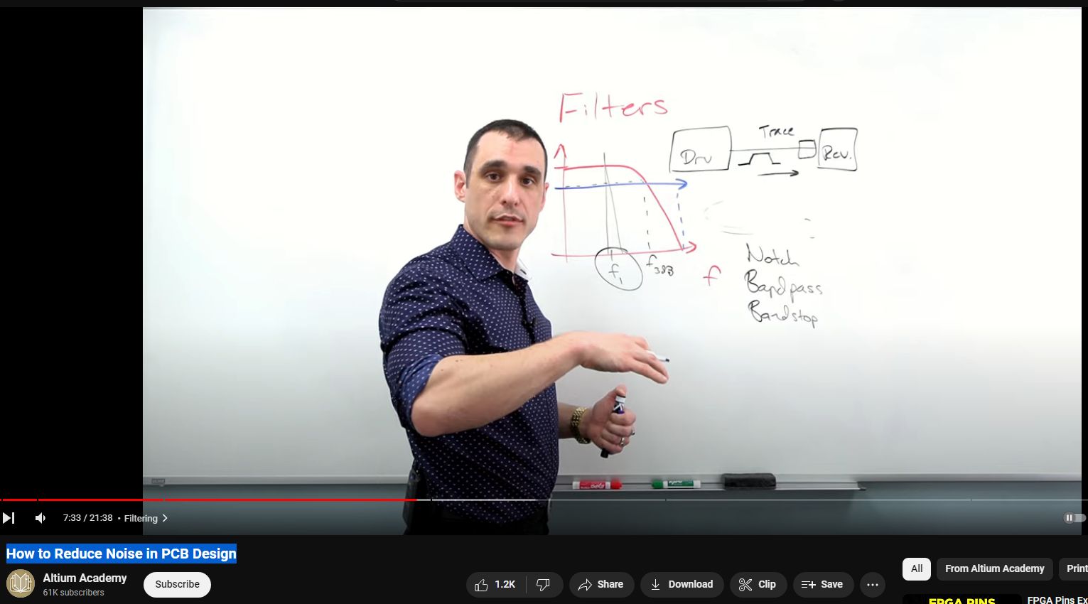
And if you graph a transfer function for a filter,
H is gonna be as some function of frequency,
and there will be some curve here, okay?
And let’s just take a low-pass filter
just as an example,
which transfer function basically looks like this.
Now, the transfer function tells you the output
versus the input voltage,
and that’s equal to my transfer function
as a function of frequency.
So what this is telling you is that if I have a signal
and it’s operating at this frequency, f1,
and let’s just say, it’s just a spike here.
So it’s just this one signal operating at f1.
What this transfer function is telling you
is that it’s gonna allow all of the power in f1
to reach the destination.
Now, everything above this f3dB roll-off,
everything above that is gonna get heavily attenuated
and will essentially get removed from the interconnect.
And so the point of drawing out a transfer function
is to tell you that you can’t just pick random filters
and pair them up with your particular interconnect
and then expect to remove every noise source.
So you should actually look at what the noise is
on an oscilloscope, or even better,
on a network analyzer or on a signal analyzer,
and you can actually pick out the frequencies
that you need to eliminate.
So if you just wanna transfer one specific frequency
down the interconnect,
maybe you have a driver component,
and you have your trace,
and then you have your receiver,
somewhere along this trace,
it’s picking up some noise.
So if you already know
the frequencies involved in this noise source,
then you can design a filter
and put it somewhere here, usually near the receiver,
for this signal that is going to only allow this signal
while removing this particular noise source.
So your filter options are usually something
like a notch filter.
That’s gonna remove specific frequencies.
You could also have a bandpass filter,
so meaning it’s only gonna allow
the frequency that you want,
so in this example, f1, while removing everything else.
You could also have a band-stop filter.
So maybe just in this example
you have another frequency, f2,
that’s originating from your noise source
and reaching your trace.
And then in that instance,
the band-stop filter could target f2,
while having zero attenuation at f1.
Filters are useful for targeting specific frequencies.
Now, if this were, say, a digital interconnect
and we had a signal that was a digital signal
and it’s traveling this direction
from the driver to the receiver,
well, should we use filtering?
Well, the answer is no,
we actually shouldn’t be using any kind of filters.
The reason we shouldn’t be using any kind of filters
is because, generally, with filtering components
that are operating in practical frequency ranges,
you’re actually gonna attenuate a lot of this digital signal
and you could distort it to the point
where it doesn’t trigger the receiver properly.
And the reason for that
is because a digital signal does not have all of its power
concentrated at one frequency,
its power is actually concentrated,
well, theoretically, all the way out to infinity.
Usually, the cutoff for our digital signal bandwidth
is gonna be very high.
And so we’ve talked about this before,
that actually relates to the rise time.
So if you go back and watch one of our videos
on digital signal bandwidths,
we’ll put the link in the description,
that will tell you why the power spectrum
of a digital signal spans out so far
into the high-frequency range.
And you can’t remove high frequency noise
with something like a low-pass filter as I’ve shown here.
Next, shielding,
what exactly is shielding?
Well, shielding, as I said before,
is pretty much anything that you can use
to create, essentially, the equivalent of a Faraday cage
around your components.
Now, no Faraday cage is perfect,
and you could basically go just as heavy as you want
and make a totally enclosed
shielded metal enclosure around your board
and to try and eliminate any sources of outside noise.
And you could do that,
but you may not be successful.
There are actually other things
that you’ll wanna do in your PCB
rather than just defaulting to shielding
to try and solve all your noise problems.
So just as an example,
let’s take a look at our cross section of a PCB.
And let’s just say for a moment
that I have an integrated circuit here
and it’s receiving a lot of noise from some outside source.
Well, the guys that claim
that you should always use shielding
around these types of components
will basically put some vias around here.
And what they’ll do
is they’ll go find a big metal shielding can
that basically encloses this entire component.
And so the idea here is that
if this component is emitting a lot of noise,
the shield is then gonna block this.
And then what they’ll do
is they’ll attach this to some pads,
they’ll connect it to ground,
usually on the next layer,
and then that basically creates a totally enclosed cage
that prevents any noise from escaping this component
and possibly reaching other circuits.
Vice versa, it also prevents any noise from out here
from entering inside the cage up to very high frequencies
and then interfering with any of the operation
of this component
or any of the other connections that it makes
that are inside of this cage.
So that’s kind of the idea behind shielding.
And people will go to various lengths
to try and create a similar structure
around different elements in a PCB.
So if you’ve seen any of my presentations
on high-frequency design,
one structure that I describe
is actually called a substrate-integrated waveguide
where you essentially shield a signal
inside to the substrate
by enclosing it on all four sides
with copper planes and vias.
It’s essentially the same thing
as like a grounded coplanar waveguide.
Coplanar waveguides, speaking of the devil,
do the exact same thing.
So let’s say that you have your PCB here
and you want to create a coplanar waveguide,
well, what you do is you basically have a trace
being routed like this,
you have some copper pour,
this is ground,
this is ground,
and then you have a bunch of vias lined up along here.
This essentially creates some shielding
by enclosing this trace as much as possible
by grounded copper,
so that if there’s any noise that comes in here,
it has very difficult for this noise
to induce a signal inside of this trace
and create some noise that then gets read out
by a receiving component.
So that’s kind of the idea behind shielding,
is basically to just block noise.
The reality is that shielding is kind of seen
as one of those things that you are just gonna have to do
on some components,
and that’s not really true.
If you do the layout correctly,
usually you don’t have to do things
like adding these shielding cans.
And there are variations of shielding cans
that you can actually implement on the enclosure,
not just on the PCB.
So there are different shielding materials
like meshes that you can put inside your device enclosure.
There are like shielding compounds or gaskets
that will absorb electromagnetic radiation
and will prevent it from entering or leaving the enclosure.
Those are other options.
All of that stuff is useful in different contexts,
but you should always start
by creating the board correctly first.
And if you do that,
then you’re gonna eliminate the need for shielding.
So when I say create the board correctly
or create the stack up correctly,
what exactly does that mean?
Well, let’s just look at an example here.
Let’s say that this is our noisy component
or our noisy circuit.
Let’s say it’s a power regulator.
And we’ve got another trace over here,
and this trace is receiving some noise from this circuit.
Well, there are a few things that you can do
to try and reduce how much noise couples from this circuit
over to this trace
that don’t involve putting any shielding around here.
So one option, if we don’t have this shielding,
is to reduce this coupling strength
between these two circuits, right?
So we’ll have some Cm here,
so that’s our mutual capacitance,
and then some Lm, that’s our mutual inductance.
So we’ve got two levers that we can pull
to try and eliminate the noise coupling
between these two circuits.
Those are, number one, to take the distance here,
so d, and increase it.
So spacing things out is always gonna reduce noise
every single time.
It will always reduce the noise
that gets coupled from here over to here.
So that’s your first lever you can pull,
is just space stuff out.
The other thing that you can do is
if you have a ground plane on the next layer,
which you usually should,
you can take this height,
so this distance between the trace and the ground plane,
and you can reduce it, okay?
So bring the ground closer to the trace
that’s being affected,
and that will also reduce these parasitic capacitance
and parasitic conductance values.
So just recently we did another video on parasitics,
where we actually looked at the graph
that shows what happens when you take this ground plane
and you move it closer to the circuit
that’s being affected by noise.
It actually reduces these coupling capacitances
and inductances,
and that’s gonna reduce the strength of noise
that couples from this circuit over to this circuit.
Now, let’s just suppose that the noise source over here
that you’re about to couple into this trace here
is at a specific frequency.
So maybe this, instead of a power regulator,
is some sort of analog circuit,
and the analog signal is harmonic,
so it’s operating at a single frequency.
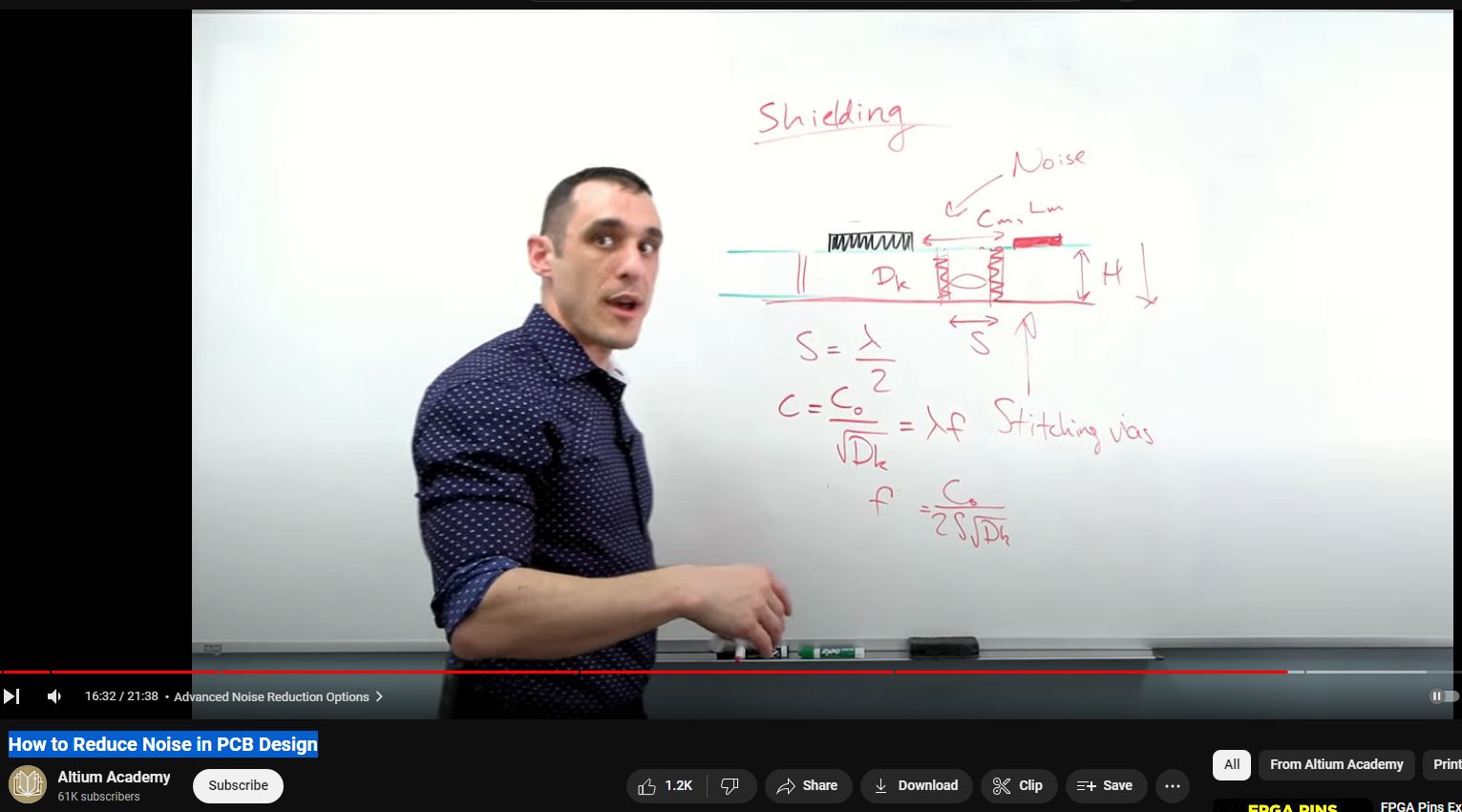
So what you could do is you could put stitching vias
around this circuit.
So putting stitching vias around this trace is effective
if the vias are sized properly.
So don’t just pick some random value
like two-millimeter spacing or whatever
and expect that that’s always gonna work
for every frequency.
So we discussed in a previous video
the role of stitching vias in copper pour
and how they can actually contribute to resonances
that aid noise transfer between two circuits,
or how they suppress resonances
and prevent noise transfer between these two circuits.
And so they do that
by creating a resonant cavity between them.
So let’s just say for a moment that I’ve got two vias here
and they’re separated by some distance S.
Whenever S is equal to half a wavelength,
where this wavelength is the wavelength
inside of this particular structure
associated with the decay of the substrate,
then you will have a strong resonance
that builds up in this cavity,
and that strong resonance could aid noise transfer
into this interconnect,
which could then get read out by the receiving component.
So, what exactly is the wavelength
that we’re talking about here,
the half wavelength?
Well, if you remember your basic physics,
the speed of light inside of the substrate here
is just the speed of light in vacuum
divided by the refractive index or the square root of Dk.
And then that is equal to the wavelength
inside of this structure multiplied by the frequency.
So if we just substitute in,
Lambda equals 2S into this equation,
we get f times 2S is equal to C sub zero
over square root of Dk.
Solve for f.
I get f is equal to 2S square root of Dk in the denominator
divided by speed of light in vacuum, okay?
So you can look this up in any old textbook.
S is something that you chose
when you set up your stitching vias.
DK,
that’s just the dielectric constant
for your substrate material.
So this tells you the frequency
that is going to build up a strong resonance
between these two vias.
And so you would like to prevent that.
Because whenever you have a strong
electric and magnetic field built up inside this structure,
that strong field could then couple noise
into a nearby interconnect,
and that’s going to actually increase noise transfer
between these two circuits.
So if you space this out properly,
you will actually prevent all lower-level frequencies,
so frequencies less than this,
from building up these strong resonances
and then coupling noise into this circuit.
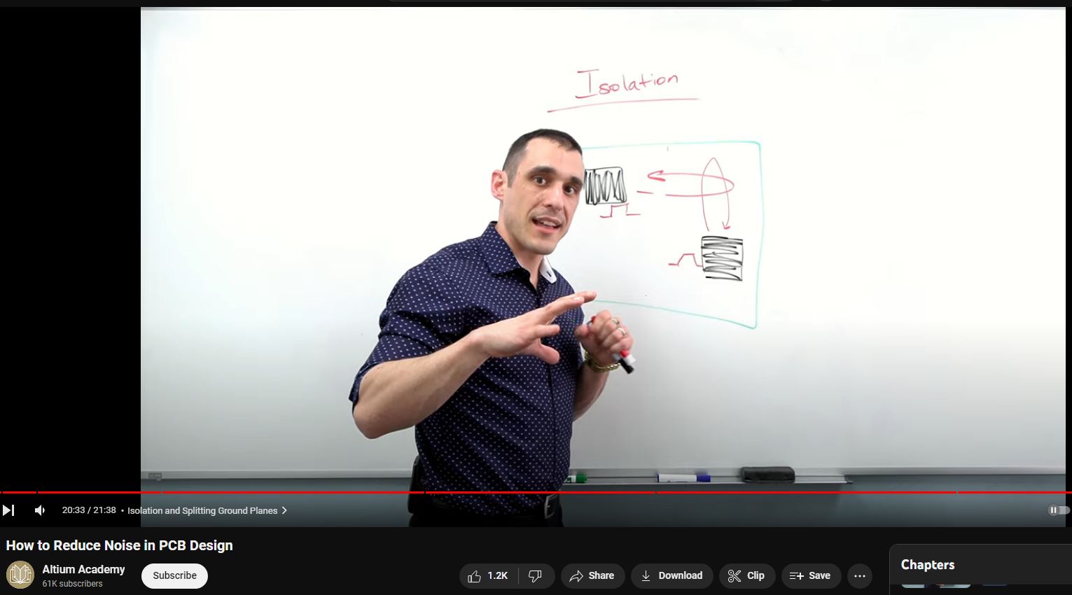
All right, last but not least, isolation.
So, what does isolation mean?
Well, let’s just look at an overhead view of a PCB,
just kind of as an example.
I could have, let’s say, a circuit here,
and I wanna prevent it from coupling any noise
into a nearby integrated circuit
and all of its traces and everything.
Isolation says that you essentially prevent the return path
associated with any of the traces
and any of the signals moving around in this circuit
from interfering with the return paths of,
let’s say, this circuit over here.
So this is essentially the counterpart of noise coupling
that I was referring to
when we were talking about shielding.
Now, generally, when people talk about isolation,
this is where you’re gonna see
that 30-year-old design guideline come up that says
you should start splitting up ground planes.
And I still, to this day, see new articles coming out
that say you should split up ground planes
in order to prevent isolation from,
let’s say, a signal over here
from creating a return path that then interferes
with a different signal over here.
It is true that you do wanna prevent the return paths
from appearing to superimpose on each other
and then create noise transfer between these circuits,
however, splitting up the ground plane
and doing something like this
is really not the right way to do it.
So the issue here is that you need to take note
of where your return paths exist
and prevent return paths from crossing each other.
So just as an example,
if I have a return path that exists here
and I have another return path that exists here
along a circuit,
it’s possible that
if there’s no ground plane
or any ground separating these,
that these signals could couple noise into each other
and you essentially have a form of crosstalk
that would then be read out
at whatever IOs you’re dealing with.
That’s essentially what could happen in this circuit.
And basically just changing the layout
is probably gonna fix this problem.
So maybe moving this over, moving this up,
and then re-engineering where you put the actual IO port
or whatever the receiving component is
that needs to interact with these two chips,
that is actually gonna solve this problem for you
without having to do anything
like splitting up a ground plane.
So pretty simple.
I’ve been told in the past that I talk a little too much
about not splitting up a ground plane.
And for most designs,
you don’t need to split up a ground plane,
especially, if you’re dealing
with the standard set of digital buses.
So let’s say you’re doing like a microcontroller board.
You need to access the SPI, I2C, UART,
whatever other standard digital buses are on there.
So if you’re dealing with that case,
save yourself a lot of headache,
go with a solid ground plane.
Don’t try and split it up,
and practice good layout practices
and learn how to track return paths,
and you’re gonna be in good shape,
you’re gonna prevent a lot of your noise problems.
Now, there are some specialty cases
where you actually might need to split up the ground plane,
because the frequencies involved are such that
that is the only way you’re gonna be able
to provide any kind of isolation.
So I’ll give you one great example
that I was just recently reminded about
from someone that works at another company,
which is precision DC measurements.
So with highly precise DC measurements,
again, in that case, the return paths are such
that you actually kind of have no choice,
you may have to split up the ground planes
in order to provide the isolation you need.
Some audio systems,
it’s actually desirable to do this
because they may have a digital section on the front end,
and that’s what the user interacts with,
and there’s gonna be the standard digital buses.
Those could then couple noise into your audio section.
Those audio frequencies are such
that they need to be confined from the digital stuff.
And one of the easy ways to do that
is by splitting a ground plane.
However, those are the exceptions,
those are not the rule.
Give yourself a reason to split the ground plane
if you think you need to do it.
Come up with a compelling reason and then do it.
Don’t split it first
and try and find a reason to use a full-ground plane.
All right, everybody, thanks for tuning in.
And hopefully this gives you some strategies
that you can think about
to deal with your own noise problems in your PCB,
should you ever find them.
Now, one thing I didn’t mention,
which I probably should have mentioned at the beginning,
is if you do have noise problems,
try and track down what the actual source is,
that’s going to give you a reference to try and figure out
how you can actually approach this
and what strategy is gonna be best
for your specific noise problem.
All right, thanks again, everybody.
Watch this video at 2x speed for maximum effect.
See Also
Parasitic capacitance refers to unintended or unwanted capacitance that exists between different conductive elements in an electronic circuit. These capacitances can arise due to the physical proximity of conductors, traces, or components on a PCB, as well as the intrinsic capacitance of semiconductor devices and interconnects.
Here are some key points about parasitic capacitance:
1. **Nature of Parasitic Capacitance**: Parasitic capacitance is an inherent property of electronic components and interconnections. It occurs due to the electric field between two conductors separated by a dielectric medium, which can be air, PCB substrate material, or insulating layers.
2. **Effects on Circuit Performance**: Parasitic capacitance can have several effects on circuit performance, depending on the specific application. In high-frequency circuits, parasitic capacitance can degrade signal integrity, cause signal distortion, and increase power consumption. In analog circuits, it can introduce coupling between different signal paths, leading to crosstalk and noise.
3. **Sources of Parasitic Capacitance**:
– Between PCB traces: Adjacent traces on a PCB can form parasitic capacitance, especially when they run parallel to each other for an extended distance.
– Between components: Components placed close together on a PCB can have parasitic capacitance between their leads or terminals.
– Within semiconductor devices: Parasitic capacitance exists within semiconductor devices due to the intrinsic capacitance between different layers of the device structure, such as between the gate and the drain in a MOSFET.
4. **Minimizing Parasitic Capacitance**:
– Proper PCB layout: Careful PCB layout design, including trace routing, component placement, and layer stackup, can minimize parasitic capacitance. Techniques such as reducing trace length, increasing trace separation, and using ground planes can help mitigate parasitic effects.
– Component selection: Choosing components with lower parasitic capacitance specifications can help reduce overall capacitance in the circuit.
– Shielding and isolation: Using shielding techniques or isolation barriers between sensitive circuit sections can help reduce parasitic capacitance coupling.
– Signal termination: Proper signal termination techniques, such as matching impedance and using termination resistors, can help mitigate the effects of parasitic capacitance in high-speed digital circuits.
5. **Simulation and Analysis**: Parasitic capacitance can be analyzed and simulated using specialized EDA (Electronic Design Automation) tools. These tools allow designers to predict and optimize the effects of parasitic capacitance on circuit performance during the design phase.
Overall, while parasitic capacitance is unavoidable in electronic circuits, careful design practices and mitigation techniques can help minimize its impact on circuit performance and ensure reliable operation.